
AC-powered LEDs Could Cut the Cost of Lighting
aside.inlay.xlrg.XploreFree
font-relatives: “Ga”, serif
border-width: 4px
border-top: strong #888
border-base: strong #888
padding: 10px
font-size: 19px
font-excess weight: bold
text-align: center
span.FreeRed
shade: red
text-remodel: uppercase
font-relatives: “Theinhardt-Medium”, sans-serif
span.XploreBlue
shade: #03a6e3
font-relatives: “Theinhardt-Medium”, sans-serif

Engineers at Pennsylvania Condition College have shown a realistic way to integrate gallium nitride LEDs and their power offer circuits on to the identical chip using sector-conventional producing processes. The outcome is a lights chip that operates instantly from the AC energy equipped by a wall outlet, with no need for the intermediate move of converting the energy to minimal-voltage DC on separate silicon chips and other parts.
The Penn Condition engineers explain the perform in IEEE Transactions on Electron Devices.
In accordance to Penn Condition engineering professor Jian Xu, who led the investigation, integrating the LED’s driver procedure on to the gallium nitride chip could lower the value of producing LED lights as well as the value of maintaining that lights. As considerably as 60 p.c of the value of an LED bulb comes from the driver electronics, he suggests. And for the reason that individuals silicon driver electronics are generally fewer sturdy than gallium nitride, they have a tendency to are unsuccessful ahead of the LED alone does.
The current driver circuits in an LED lamp complete 3 main capabilities: They transform the AC to DC (rectification), sleek out ripples in the resulting DC, and lower the voltage to a additional LED-welcoming amount.
The on-chip driver procedure that Xu’s group built only performs the initial function (rectification) even though reducing the want for the 3rd (reducing the voltage).
The driver consists of 4 Schottky barrier diodes (SBDs) organized into a bridge rectifier circuit. SBDs are diodes shaped by the junction between a metallic and a semiconductor. They are popular in power electronics, for the reason that they have a minimal ahead voltage drop. Gallium nitride is an especially great material with which to make them, because it has a large breakdown voltage that prevents the stream of latest in the reverse way.
In purchase to get the ideal voltage to the LEDs, the products are crafted as an array and cascaded in a chain of 22 to forty pixels per rectifier. In that way, the whole voltage drop is the a hundred and ten-120 V from the wall socket, but each individual LED pixel sees only a couple volts.
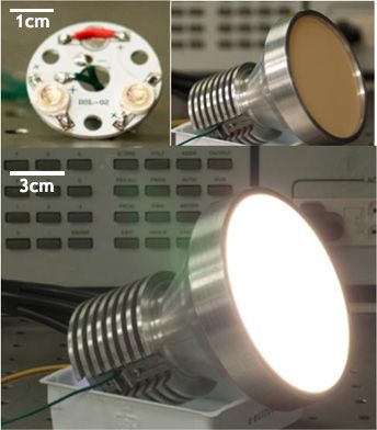
A white LED lamp using the prototype integrated chip created a respectable 89 lumens per watt. Even so, for the reason that the SBD bridge outputs a rectified model of the AC input alternatively than a about continual voltage, the LED has a 120-hertz flicker, which would make it additional acceptable for out of doors lights purposes such as lamps for parking plenty and roadways, the place minimal routine maintenance value is crucial but gentle high quality is fewer important.
Integrating an LED light’s driver circuits could possibly feel like an obvious thought, but it’s been out of attain until eventually not too long ago. “Gallium nitride is a relatively new material procedure,” Xu suggests. “The engineering has turn into experienced only not too long ago, that is why integration on a solitary chip is a pretty new thought.” Previous tries have required the use of possibly specialized LED constructions or producing processes that have been too advanced to scale up or have been too harmful to LED efficiency.
Fixing that past dilemma was the vital to Xu’s lab’s achievement. In silicon chip producing, etching absent material to form products can be finished with “wet” chemistry, such as treatment method with hydrofluoric acid. But gallium nitride is too hard for that to perform, explains Xu. So alternatively “dry etching” —inductively coupled plasma etching—is utilized. Regretably, that approach can go away efficiency-sapping problems on the surface area.
“We invested two several years trying to lower problems using a blended etching system,” suggests Xu. Although damp etching isn’t sturdy more than enough to take out considerably of the semiconductor surface area, supplied time, it can assistance take out the defective layer still left by dry etching. His crew at some point hit on a sequence of dry etching and damp etching that created minimal-defect, large high quality products. Even superior, this “cyclic etching” procedure could be utilized to enhance the efficiency of microLEDs for displays, in accordance to Xu.